
 MENU
MENU 

$1.8M to develop room temperature, controllable quantum nanomaterials

An effort to create quantum semiconductors that operate at room temperature has been awarded $1.8 million by the National Science Foundation. The success of the University of Michigan team could lead to the integration of quantum information and communications technologies with conventional computers—as well as advances in high-precision sensing and more sustainable UV lamps for sterilization and air purification.
“By demonstrating the controlled synthesis of such quantum nanomaterials, utilizing industry-standard processing tools, we hope to establish the material platform for scalable, next-generation quantum technology,” said Zetian Mi, a professor of electrical engineering and computer science and principal investigator of the project.
Gallium nitride has been widely hailed as the future’s silicon, and its properties can be tuned by replacing some of that gallium with boron, aluminum and indium—cousins of gallium in the same column of the periodic table. These materials are widely used in LEDs and in power electronics. But they can also support what are known as extreme quantum-dot arrays.
Quantum dots are groups of atoms that behave like a single atom, absorbing and emitting light at single wavelength or a few distinct wavelengths. Extreme quantum-dot arrays differ from conventional quantum dots in that they are perfectly ordered and emit light identically. Researchers believe that they could offer new levels of control over quantum light emission and interactions between quantum dots used as qubits, or quantum bits. Unlike conventional computer bits, which can only be a 1 or a 0, qubits can represent both states at once.
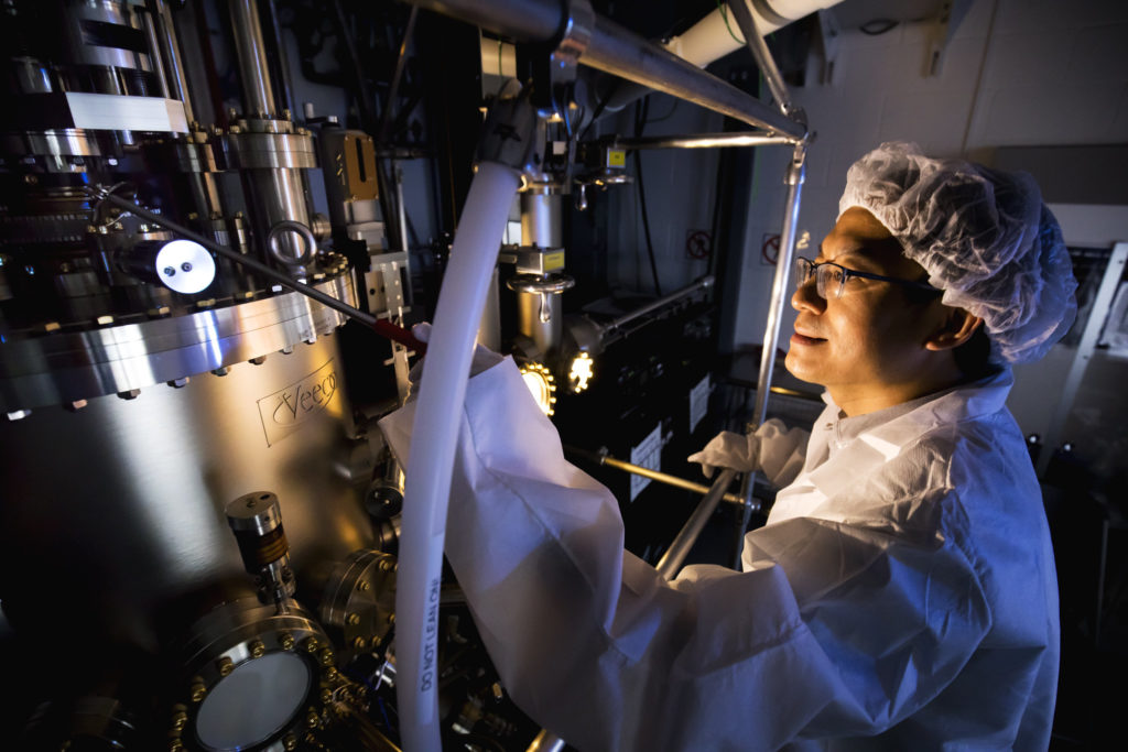
But so far, researchers haven’t been able to build perfectly ordered materials, controlling the location and size of each dot. This is necessary for controlling how the quantum dots interact when used as qubits. Mi believes that his team can overcome this through a process called ultrahigh temperature molecular beam epitaxy, which enables his team to build up the semiconductor one layer at a time, carefully controlling each layer.
“When you make these quantum nanostructures, new operational principles come alive,” said Mackillo Kira, a co-principal investigator and professor of electrical engineering and computer science.
Because quantum nanomaterials differ from both classical semiconductors and conventional quantum materials, Kira is leading the arm of the project developing a systematic quantum theory that will predict their behavior. This theory will enable researchers to figure out the available quantum states in these nanostructures, their light emission properties and their capacity for quantum entanglement.
When you make these quantum nanostructures, new operational principles come alive.
Prof. Mackillo Kira
The light emission is useful for reading and writing quantum information, but it can also be used directly for efficiently producing UV light. At present, UV sterilization and air purification technology typically relies on mercury lamps, which contain toxic materials and produce a lot of waste heat. Mi believes quantum nanomaterials could make UV-C lamps safer and 100 times more efficient than what is currently available in the far UV-C.
“This material is ideally suited for UV optoelectronics, including UV LEDs for disinfectant applications,” said Mi. “Broadly speaking, 200 to 280 nanometers is very important for disinfection purification applications. But there is no viable way to do that efficiently using conventional semiconductor technology.”
Beyond UV lamps, Kira is particularly interested in quantum computing and communications.
“We’re talking about controlling the energy of light, and then what type of light is emitted which is also critical for quantum information applications, such as moving information long distances, quantum processing, information security, or high-resolutionly sensitive sensing and detection,” said Kira.
Mi’s group will use the theory to inform how they build the semiconductors to get the desired quantum properties. Then, researchers specializing in materials characterization will test the new materials to confirm their reliability, and by extension, the underlying theory.
“If we can make a few entanglement-based demonstrations, based on the new materials, that’s a big step forward,” said Kira. “That would be a founding moment of making semiconductors quantum-ready.”
In addition to Mi and Kira, key members of the team include co-principal investigators Theodore Norris, the Gerard A. Mourou Professor of Electrical Engineering and Computer Science, and Parag Deotare, an assistant professor of electrical engineering and computer science, who will test and evaluate the materials. In addition, Manos Kiopakis, an associate professor of materials science and engineering, will help with the design and modeling of gallium nitride structures. Industrial partners Sandia National Lab and the Air Force Research Lab bring extensive experience in materials characterization.
The project is called “III-nitride Monolayers and Extreme Quantum Dots.” It is part of the Materials Genome Initiative, a federal multi-agency initiative for discovering, manufacturing, and deploying advanced materials twice as fast and at a fraction of the cost compared to traditional methods.
Some IP related to this work was licensed to NS Nanotech, Inc., which was co-founded by Mi. The University of Michigan has a financial interest in NS Nanotech.
Early research undertaken related to this project was partially funded by the W.M. Keck Foundation. The foundation’s funding helped with essential ‘proof of concept’ gains.